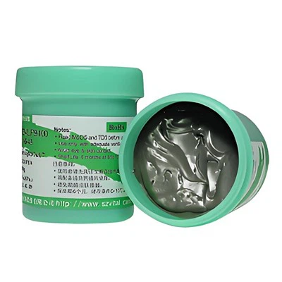
LED SMT Solder Paste
This product consists of two parts: flux and alloy powder. The flux system uses a rosin-based formula, prepared by adding activators, thixotropic agents, solvents and other components. The alloy powder is Sn43Pb43Bi14 ternary alloy, manufactured through gas atomization process, with sphericity above 90% and oxygen content controlled below 300ppm.
The melting point of this solder paste is 143℃, which is 40℃ lower than the 183℃ melting point of Sn63Pb37 eutectic solder. This characteristic makes it suitable for LED product assembly soldering, heat-sensitive component packaging, and PCB secondary mounting. The post-soldering residue is non-ionic type and requires no cleaning.

Product Features
Flux System
The activators in the flux decompose during heating, and the generated acidic substances react with metal oxides to remove the oxide layer from the pad and component lead surfaces. Meanwhile, the activators reduce the surface tension of molten solder, allowing the solder to spread on the pads. The addition of thixotropic agents enables the solder paste to maintain its shape when stationary and flow when subjected to shear force. This characteristic ensures operability during printing and placement processes.
Printing Performance
The viscosity of solder paste is set in the range of 110-180Pa.s, which is compatible with stencil printing process. During printing, solder paste is deposited on pads through stencil apertures and maintains the aperture shape after demolding. The evaporation rate of solvents in the solder paste is controlled so that viscosity change does not exceed 15% within the 8-hour stencil life cycle.
Post-Soldering Condition
After soldering is complete, the solder joint surface shows metallic luster, and solder coverage on pads reaches above 95%. Flux residue appears transparent or light yellow, with residue amount less than 2% of total paste weight. The surface insulation resistance of residue measures no less than 1×10¹⁰Ω under normal temperature and humidity conditions.
Alloy Composition
The addition of Bi element changes the phase diagram structure of SnPb binary alloy, forming a ternary eutectic point and lowering the alloy melting point. When Bi content is 14%, the alloy melting point drops to 143℃. Bi segregates at grain boundaries during solidification, forming a network distribution, which affects the creep resistance of solder joints. Sn and Pb form a solid solution, providing the matrix structure of solder joints.
Reflow Soldering Process
The reflow soldering temperature profile is divided into preheat zone, soak zone, reflow zone, and cooling zone. The preheat zone heating rate is controlled at 1-3℃/s, the soak zone temperature is set at 120-140℃ and maintained for 60-90 seconds, the reflow zone peak temperature is set at 160-180℃, and time above liquidus is controlled at 30-60 seconds. The cooling zone cooling rate does not exceed 4℃/s.
Scope of Application
LED Display Products
Including SMT mounting processes for indoor and outdoor LED display modules, LED dot matrix modules, LED digital tubes and other products. Suitable for products with lamp bead spacing ranging from P1.0 to P10. For products with spacing less than P2.0, T4 powder diameter models are recommended to reduce solder ball generation.
LED Lighting Products
Including soldering of LED lamp boards, LED power boards, and LED driver modules. Suitable for different substrate materials such as aluminum substrates, fiberglass boards, and ceramic substrates.
Heat-Sensitive Component Packaging
For components with temperature tolerance upper limit below 200℃, such as certain sensors and plastic-packaged devices, this product can be used for low-temperature soldering to avoid damage to devices caused by high temperature.
Secondary Assembly Process
When performing repair soldering or adding components on circuit boards that have completed primary soldering, using this product can avoid remelting of existing solder joints.
Technical Parameters
| Item | WTO-LED-F | WTO-LED-F/T4 | WTO-LED-2F |
|---|---|---|---|
| Alloy Composition | Sn43/Pb43/Bi14 | Sn43/Pb43/Bi14 | Sn50/Pb45/Bi5 |
| Melting Point | 143℃ | 143℃ | 160℃ |
| Halogen Level | R0L1 | R0L1 | R0L1 |
| Powder Diameter | T3 (25-45μm) | T4 (20-38μm) | T3 (25-45μm) |
| Viscosity | 110-180 Pa.s | 110-180 Pa.s | 110-180 Pa.s |
| Metal Content | 89.70±0.5% | 89.70±0.5% | 88.00±2.0% |
| Flux Content | 10.30±0.5% | 10.30±0.5% | 10.30±0.5% |
| Surface Insulation Resistance | ≥1×10¹⁰Ω | ≥1×10¹⁰Ω | ≥1×10¹⁰Ω |
| Printing Speed | 20-100 mm/s | 20-100 mm/s | 20-100 mm/s |
| Stencil Life | 12H | 12H | 12H |
| Storage Temperature | 0-10℃ | 0-10℃ | 0-10℃ |
| Shelf Life | 6 months | 6 months | 3 months |
Parameter Notes
T3 powder diameter refers to powder diameter distribution in the 25-45μm range, suitable for printing conditions with stencil thickness above 0.12mm and aperture area greater than 0.4mm². T4 powder diameter distribution is in the 20-38μm range, suitable for fine-pitch printing. R0L1 indicates that halogen content complies with low-halogen requirements in IPC J-STD-004B standard, with bromine content below 0.05% and chlorine content below 0.05%.
Storage and Usage
Solder paste must be refrigerated and stored in 0-10℃ environment. Freezing is prohibited. Before use, remove from refrigerated environment and allow to return to room temperature for at least 4 hours. Do not open during the warming period. After opening, stir for 3-5 minutes to make the solder paste uniform. Opened solder paste should be used within 24 hours. Solder paste on the stencil should be stirred every 30 minutes.
0-10℃
Storage Temperature
4+ Hours
Warming Time
24 Hours
Use After Opening
Hot Tags: led strip solder paste, China led strip solder paste manufacturers, suppliers, factory, High reliability Zero halogen Solder Paste, LED Panel Solder Paste, LED Strip Solder Paste, Photovoltaic Solder Paste, Semiconductor Solder Paste, solder paste