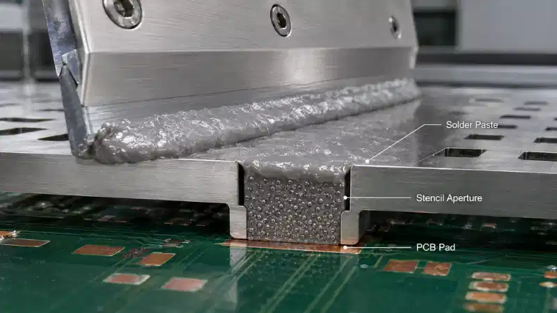
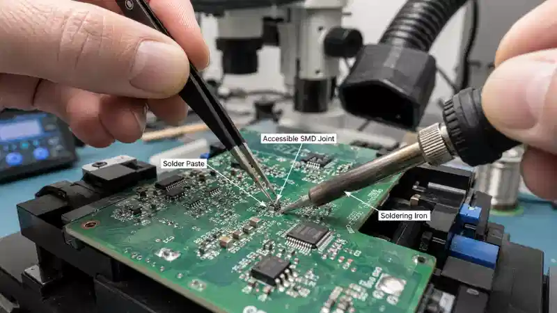
Can you use solder paste with a soldering iron? Yes, but the method is most practical for surface-mount components with visible, accessible terminations that can be heated and inspected directly.

It can be useful for prototypes, small repairs and low-volume work without a full stencil-printing and reflow line. It is not a universal replacement for reflow. Hidden joints, very fine pitch, large bottom pads and high pin counts require tighter control of solder volume, heating and inspection.
The basic decision is straightforward:
- Use solder paste with an iron only when each joint is accessible and controllable.
- Use solder wire when feeding solder to one exposed joint is simpler.
- Use hot air or controlled reflow when several leads should reach temperature together.
- Use a mini-stencil or controlled dispenser when repeatable deposit volume matters more than freehand convenience.
Readers who need a general introduction to the material can begin with what solder paste is and how it works.
Can You Use Solder Paste with a Soldering Iron?
Electronics-grade solder paste contains solder alloy powder suspended in a flux vehicle. With suitable heating, the flux activates, the powder particles melt and the metal coalesces into a solder joint.
A soldering iron can provide enough local heat for some exposed SMD joints. The main limitation is heat distribution. An iron heats a small contact area, while conventional reflow heats the component and its joints more evenly.
Uneven local heating can create several problems:
- The flux may activate too early or become thermally degraded before all particles coalesce.
- One termination may melt before the other, allowing the component to move.
- Several leads on the same package may receive different thermal exposure.
This method therefore requires control over paste volume, component position and heat transfer. A paste formulated for one deposition or reflow process may not behave identically when applied manually and heated rapidly, so the product technical data sheet remains the starting point.
Which SMD Packages Are Suitable?
Reasonable Starting Candidates
The following are practical examples when their terminations are visible and the operator has adequate magnification:
- 0805 and 1206 resistors or capacitors;
- 0603 components after practice on larger packages;
- SOT-23 transistors and similar devices;
- LEDs and diodes with exposed end terminations;
- wider-pitch SOIC packages;
- individual gull-wing leads that can be reached from the side.
These are starting examples, not acceptance criteria. Pad size, board finish, copper area, component thermal mass and operator access can change the result.
Packages That Need Better Process Control
Another process is usually more suitable for:
- QFN or DFN packages with bottom terminations;
- BGA or LGA packages;
- components with large hidden thermal pads;
- very fine-pitch QFP or TSSOP devices;
- connectors with hidden or closely spaced contacts;
- assemblies that cannot be inspected adequately after soldering.
A package can look correctly positioned while still containing an open, bridge or insufficient joint underneath. When controlled dispensing is required, the broader guide on choosing a solder paste application method explains when manual placement, dispensing or stencil printing is more appropriate.

Solder Paste, Wire, Hot Air or a Mini-Stencil?
The best starting method depends on the joint geometry and the level of process control required.
| Situation | Practical Starting Method | Main Reason |
|---|---|---|
| One accessible chip component | Paste with an iron or controlled hot air | Small, visible deposits can be positioned and inspected |
| One exposed lead or terminal | Solder wire | Direct feeding may provide simpler metal control |
| Through-hole component | Solder wire | Paste usually offers little practical advantage |
| Wider-pitch SOIC prototype | Paste with controlled local heating | Leads remain visible and can be checked individually |
| Fine-pitch multi-lead package | Mini-stencil and controlled reflow | Deposit consistency becomes critical |
| QFN, DFN, LGA or BGA | Controlled reflow and suitable inspection | Joints are hidden |
| Several identical boards | Mini-stencil or controlled dispenser | Repeatability matters more than freehand speed |
| Joint already contains enough solder | Flux and controlled reheating may be sufficient | Additional solder metal may not be required |
For a wider material comparison, review the differences among solder wire and other solid solder forms.
Tools, Materials and Safety Checks
Prepare the process before placing paste on the PCB. A typical setup includes:
- electronics-grade solder paste;
- the product technical data sheet and safety data sheet;
- a temperature-controlled soldering station;
- a clean, properly tinned tip with enough thermal capacity for the joint;
- fine tweezers and a stable PCB holder;
- magnification;
- appropriate ESD controls;
- local fume extraction;
- solder wick for correcting excess solder;
- an approved cleaning method when cleaning is required;
- a scrap board or test coupon.
A very small needle or improvised applicator is not automatically more accurate. Deposit control depends on the paste, pad geometry and operator technique. The general solder paste application guide provides additional background on preparation and handling.
Safety Before Soldering
Read the SDS for the actual product. Use eye protection, capture fumes near the source and keep food and drinks away from the work area. Wash your hands after handling soldering materials, especially when working with lead-containing alloys. Handle boards and components using suitable ESD controls.
Jewelry solder paste is not a substitute for electronics solder paste. Alloy composition, flux chemistry, heating method and cleaning requirements may be different.
Step-by-Step Hand Soldering Method

Step 1: Verify the Paste, Alloy and Component
Confirm that the material is intended for electronics, is within shelf life and has a known storage history. Check that the alloy and flux system are compatible with the assembly, and make sure the component has visible, accessible terminations.
If the existing solder alloy is unknown, investigate the assembly specification before adding another material. The guide to common tin solder alloys for PCB assembly can help identify the alloy questions that should be answered first.
Step 2: Prepare Flat, Clean Pads
Secure the PCB and inspect the work area under magnification. Remove contamination and excessive old solder using an approved process. The component should sit flat on the land pattern before new paste is added.
Solder paste cannot repair a lifted pad, missing copper, damaged solder mask, severe oxidation, an incorrect footprint or a mechanically unstable component. Those defects require a separate repair decision.
Step 3: Apply Small, Balanced Deposits
Place paste only where solder is needed. For a two-terminal chip component, use small and similar deposits on both pads. For exposed leads, keep each deposit centered on its pad and out of the spaces between leads.
A fixed dot diameter is unreliable because pad geometry varies. The required volume depends on pad area, termination size, existing solder, paste metal loading, alloy, surface finish and desired joint geometry.
Start with less paste than appears necessary and test the deposit on scrap hardware. Removing a bridge from tightly spaced leads is usually harder than adding a controlled amount later.
Step 4: Place the Component Vertically
Lower the component with tweezers rather than dragging it across the pads. Sliding can smear paste beyond the intended area or push it into adjacent gaps.
Before heating, verify orientation, polarity, lead-to-pad alignment, paste spread, clearance from nearby pads and whether the component sits level.
Step 5: Transfer Heat Through the Pad and Termination
Use a clean, tinned tip that can contact the joint efficiently without touching neighboring parts. A very sharp tip is not always the best choice; the tip must have enough contact area and thermal capacity to transfer heat into both the pad and the component termination.
The objective is to heat the joint surfaces so the paste between them reaches its working range. Pressing the tip only into the top of the paste can activate the flux without transferring enough heat into the metal surfaces.
For a chip component, stabilize the part and heat one accessible joint until the paste coalesces and wets the visible surfaces, then move to the other side. For a wider-pitch gull-wing lead, contact the lead and pad area while observing the paste change from a grainy deposit into a continuous joint.
There is no universal tip temperature or contact time. Alloy, tip geometry, station recovery, copper area, board thickness, component thermal mass and paste formulation all affect the required heat. Use the product documentation, component limits and a validated test board to establish the process.
Step 6: Let the Joint Cool Without Movement
Remove the heat and hold the component still while the solder solidifies. Movement during cooling can disturb alignment or joint formation.
If alignment is wrong, allow the area to cool and reassess the cause instead of repeatedly reheating the joint without a plan.
Step 7: Inspect and Test
Inspect the completed joint under magnification. Look for correct component position, visible wetting of the pad and termination, bridges, open joints, solder balls, lifted pads, damaged solder mask and unacceptable residue.
Visible wetting should show that solder has flowed onto both intended metal surfaces rather than remaining as an isolated bead. A continuity test can help identify an electrical open, but it does not by itself prove that the joint has acceptable mechanical or metallurgical quality.
Do not judge the joint only by whether it looks shiny. Alloy and cooling conditions can change surface appearance. For additional inspection guidance, see solder paste inspection for PCB quality.
How Much Solder Paste Should You Apply?
The useful answer is a relationship between the deposit and the pad, not a universal measurement.
| Joint Type | Deposit Principle | Main Risk |
|---|---|---|
| Chip resistor or capacitor | Use similar deposits on both pads | Uneven volume can contribute to movement or a lifted end |
| SOT-23 | Keep paste centered on each visible pad | Excess paste can bridge closely spaced leads |
| Wider-pitch SOIC | Use small individual deposits | An uncontrolled bead can flood the gaps |
| Fine-pitch QFP | Prefer a validated stencil or dispenser | Manual variation may exceed the available spacing |
| Large exposed terminal | Match the deposit to the pad and termination | Excess solder can prevent seating or spread into nearby areas |
| Hidden bottom pad | Use a controlled pattern and reflow process | Excess volume can lift the package and cannot be checked visually |

Paste should remain predominantly inside the intended pad area before heating. When deposits cannot be repeated consistently, change the process rather than relying on greater operator concentration.
Common Problems and First Checks
| Problem | Likely Causes | First Checks |
|---|---|---|
| Solder bridge | Excess paste, smeared deposits or poor alignment | Review deposit position and component placement |
| Component movement | Uneven heating, excess paste or unstable handling | Check heat direction and component support |
| Paste remains grainy | Incomplete heating, unsuitable paste or poor thermal contact | Verify the material and tip-to-joint contact |
| Poor wetting | Oxidation, contamination, unsuitable flux or insufficient heat transfer | Inspect the surfaces and confirm paste compatibility |
| Open joint | Too little paste, poor seating or incomplete heating | Check the original deposit and termination contact |
| Lifted pad | Excess force, excessive heat or repeated rework | Stop heating and inspect the PCB damage |
| Unexpected residue | Flux chemistry or cleaning method does not match the process | Check the TDS before applying a solvent |
Flux activity and residue behavior are part of the material system. The article on choosing a suitable solder flux explains the main compatibility questions, while the comparison of flux paste and solder paste helps prevent material confusion.
Repeatedly adding paste and heat without identifying the cause can damage pads, components and nearby joints.
When Should You Stop Using the Iron Method?
Move to hot air, a mini-stencil or another controlled process when:
- paste cannot be kept out of adjacent pad gaps;
- several leads must reach temperature together;
- joints are hidden beneath the component;
- the package includes a large thermal pad;
- the component repeatedly moves before the solder coalesces;
- the finished joints cannot be inspected adequately;
- several identical boards require repeatable solder volume;
- the assembly has already received multiple heating cycles;
- the component or PCB has a narrow thermal limit.
For temperature-sensitive work, a purpose-designed material may be more appropriate than forcing a conventional paste into a narrow process window. Review the available lead-free low-temperature solder paste options only after confirming alloy compatibility and product requirements.
FAQ
Q: Can any solder paste be used with a soldering iron?
A: No. Alloy, flux chemistry, powder characteristics and the intended process window vary. Confirm the application with the product technical data sheet.
Q: Is solder paste easier than solder wire for beginners?
A: It depends on the joint. Paste can help position solder on small SMD pads before heating, while wire is often simpler for one exposed lead, a large terminal or through-hole work.
Q: Should I add extra flux?
A: Only when the process requires it. An unrelated flux can change activity, residue and cleaning requirements. First confirm the paste formulation and the condition of the surfaces.
Q: Must no-clean residue remain on the PCB?
A: Not necessarily. Cleaning may still be required for conformal coating, high-impedance circuits, appearance or reliability requirements. Follow the paste and assembly documentation.
Q: Can solder paste be stored at room temperature?
A: Storage requirements are product-specific. Follow the label and technical data sheet. The guide to solder paste shelf life and storage explains the main handling risks.
Q: Is 0603 a good package for a complete beginner?
A: It is usually easier to practice first on 1206 or 0805 components. Move to 0603 only when deposit control, alignment and inspection are reliable under magnification.
Conclusion
Hand soldering SMD with solder paste can work well for accessible components, prototypes and selected repairs. Success depends on controlling solder volume, component placement and heat transfer.
The method should not be treated as a substitute for every reflow process. Fine-pitch and hidden-joint packages require more repeatable deposition, more even heating and more capable inspection.
Start with a simple visible package, practice on scrap hardware and stop when the joint geometry exceeds what can be controlled by hand. For a paste recommendation based on package, alloy, flux, cleaning and heating requirements, use the YIHMA inquiry page or contact the YIHMA team.